Cindy Teng, Engineer at Technical Support Division

- Customer: National Taiwan University
- Industry: Educational/Academy
- Solution: Â ICM;Â Flow;Â Pack; Warp;Â Optics
The predecessor of National Taiwan University (NTU), Taihoku Imperial University, was established in 1928. NTU currently encompasses 12 colleges: Liberal Arts, Science, Social Sciences, Medicine, Engineering, Bioresources and Agriculture, Management, Public Health, Electrical Engineering and Computer Science, Law, and Life Science. It is made up of 56 departments, 112 institutes, 18 degree programs, over 50 international or university-level research centers, an experimental forest, and three affiliated hospitals.Â
Summary
The microlenses with the characteristics of thin, multi-function and array have been developed to solve the thickness issue caused by the conventional lens with multiple sets of lenses. NTU research group used Moldex3D molding analysis software to analyze the pros and cons of different runner systems to improve the flaw of loss of cold runner plastic in the conventional runner system and verify the feasibility of disk molding, to optimize the product design with simulation and analysis. The double-sided microlens array was also successfully produced on a 4-inch disk in the practical molding experiment.
Challenges
- Improve runner design, save materials, and increase yield per mold cycle
- Utilize Moldex3D to verify process feasibility, reducing time and cost associated with iterative mold trials.
- Optimize product warpage and optical properties to produce a microlens array with low residual stress, high precision, and excellent optical characteristics.
Solutions
Initially, the NTU research group utilized Moldex3D to analyze the feasibility of mold design to reduce the modification time and cost of the repeated trial mold. Based on the molding state, residual stress, and level of warpage, the relevant factors that have a higher impact on warpage and optical property was found, as well as the best parameters by adopting the Taguchi methods. Furthermore, the team compared and contrasted the injection molding (IM) and injection compression molding (ICM) processes, focusing on in-mold molding perspectives. Ultimately, they successfully fabricated a double-sided microlens array on a 4-inch disk through practical molding, with results aligning closely with simulation outcomes.
Benefits
- Increase the material usage rate from 18.8% to 66.3% by using direct gate rather than conventional fan gate
- Utilizing injection compression molding reduced shrinkage by 1.5 to 2%, further decreased to below 1.5% through Taguchi optimization.
- Verify the differences as well as pros and cons between the IM and ICM processes
- Improve the birefringence difference of product and enhance optical performance
Case Study
The development of virtual reality displays, and wearable devices is rapidly advancing nowadays and the thickness issue caused by the conventional lens with multiple sets of lenses is the first issue that needs to be solved. Therefore, the microlenses with the characteristics of thin, multi-function and array have been developed to solve this issue. Different from the use of fan gate for generating the microlens array in the past (Fig. 1), this project has developed a rapid and even microlens array molding process with a good optical property.
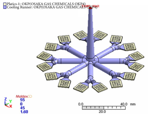
Fig. 1 The original runner design
By using a direct gate, a total amount of 48 microlens arrays could be produced in one shot (Fig. 2), significantly improving production efficiency while reducing material waste (Table 1).
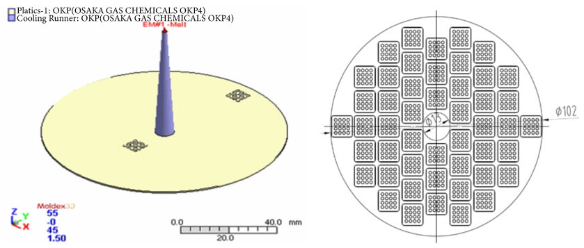
Fig. 2 Direct gate and end-product drawing
Table 1 Comparison between cold runner using fan gate and direct gate

By employing the Taguchi methods, optimal parameters for both injection molding (IM) and injection compression molding (ICM) were identified to reduce residual stress and warpage. In injection molding, melt temperature, injection speed, packing pressure, and cooling time are relatively critical factors, whereas in injection compression molding, melt time, compression gap, compression time, and compression elements have a more significant impact on packing and optical properties. The comparison of warpage and total fringed pattern between IM and ICM were shown in Fig. 3 and Fig. 4. The results indicate that ICM reduces total displacement and shrinkage and exhibits better optical performance compared to IM.
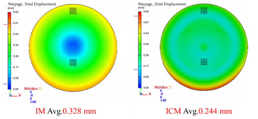
Fig. 3 The comparison of total displacement between IM and ICM
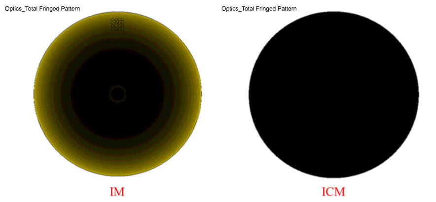
Fig. 4 The comparison of total fringed pattern between IM and ICM
The simulation results were verified by a practical molding experiment. A double-sided microlens array on a 4-inch disk was successfully produced with similar flow pattern and optical property (Fig. 5). Using OKP4 as the material, the fringed patterns were observed only near the gate area in IM, while this phenomenon was not observed in ICM. The molded microlens array showed the focus function and clear image as in Fig. 6. With the assistance of Moldex3D simulation analysis, the molding technology and efficiency of double-sided microlens array have been successfully enhanced to fulfill the requirements of high-performance, small, lightweight, and thin for the current optical industry.
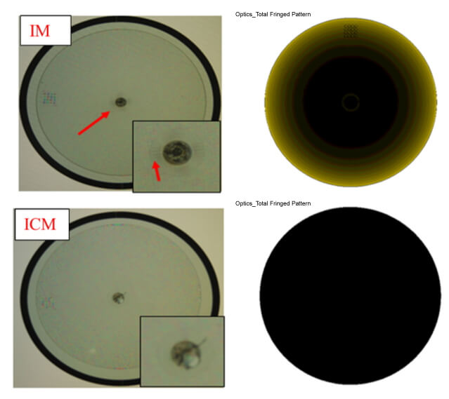
Fig. 5 The fringed pattern from simulation and actual molding
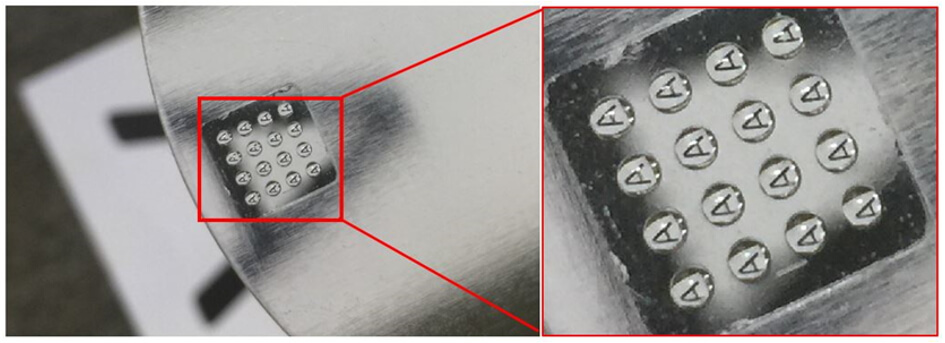
Fig. 6 Image observed by the molded microlens
Results
This study showcases Moldex3D’s proficiency in evaluating various runner designs and molding parameters. By switching to a direct gate from a fan gate, 66.3% of material can be used to produce the microlens array, which is about three times higher than the material usage rate of fan gate. Additionally, optimization parameters in both injection molding and injection compression molding substantially enhanced warpage and shrinkage. Lastly, practical molding experiments successfully produced a double-sided microlens array, yielding results consistent with Moldex3D simulations.
Granules For 3D Deep Embossing WPC Product
Virgin Hdpe Pellets,Hdpe Rigid Plastic,Recycled Hdpe Plastic Chips,Plastic Granule Hpde
Huaian Yige New Material Co., Ltd. , https://www.cnygplastic.com